by Brad Rodriguez
This article first appeared in The Computer Journal #63 (Sep/Oct 1993).
In our last episode, I supplied the design for a 6809 uniprocessor, and a simple test program to initialize the UART and exercise the serial port. Once that program is working, you can run some real debugging software: a 6809 "talker" program (Listing 1). This program lets you examine and alter memory and registers, download code, and set breakpoints. The design of the talker follows my Z8 talker from TCJ #51 [ROD91]; the few changes are documented in the listing. You can use the host program from TCJ #51 for basic memory alterations, or you can modify the host program to allow editing of 6809 registers. The source code of Listing 1, and a 6809-tailored host program, are available from the Forth Roundtable on GEnie as file 6809TALK.ZIP.
"You're either on the bus or off the bus."
- Ken Kesey, as reported in The Electric Kool-Aid Acid Test
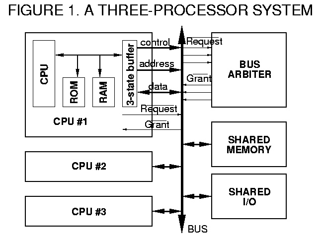
Figure 1 illustrates a simple multiprocessor system. The main bus (down the center of the diagram) is shared by all the CPU boards. Any memory or I/O board plugged into this bus is likewise shared. The bus carries address, data, and control signals between the CPUs and the memory or I/O -- just like the signals described in the previous installment which control data transfers between the 6809 and memory.
The important difference is: only one CPU board can use the bus at any time. If two CPUs try to send an address to memory simultaneously, they are likely to try driving each address line to different voltages -- with unpredictable, and possibly damaging results. The same is true of the data and control lines, of course. To avoid this, each CPU connects to the bus through a "three-state" buffer, so named because it can drive lines High (+5 volts), Low (0 volts), or not drive them at all (the third "state"). Only one CPU board can enable its three-state drivers at any time. We speak of this CPU "owning" the bus.
Obviously, we don't want the other CPUs to do nothing while they wait to use the bus. So each CPU has some "local" memory (the RAM and ROM shown for CPU #1). This memory can be accessed by the CPU chip, even when the three-state buffers are disabled. Similarly, each CPU board can have some "local" I/O. (The on-board address and data lines that interconnect the CPU chip, ROM, RAM, and three-state buffers are sometimes called the "local bus.")
So, each CPU runs normally until it tries to read or write to an "external" address, i.e., an address corresponding to one of the shared memory or I/O boards. (Each CPU decides for itself which of its addresses correspond to on-board memory, and which correspond to devices on the shared bus. This is a function of the address decoding logic.) When the CPU needs to use the bus, it asserts the REQUEST\ line, and then freezes all activity (enters a "wait" mode). When the bus becomes available to that CPU, its GRANT\ input will be asserted, telling the CPU that it can enable its three-state drivers and continue the memory cycle.
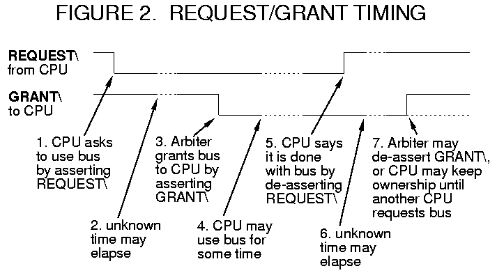
As long as the CPU continues to assert the REQUEST\ line, it keeps ownership of the bus. It is the responsibility of the CPU to de-assert the REQUEST\ line after a reasonable time, so that other CPUs may have a chance at the bus. The timing is shown in Figure 2. I use active-low REQUEST\ and GRANT\ signals; this is a matter of personal choice. Active-low signals are denoted in the text by a trailing backslash.
The problem of handling multiple simultaneous requests for the bus is left to the Bus Arbiter. I've shown this as a separate block in Figure 1. Many schemes exist for bus arbitration; I'll design a simple one in Part 3 of this series. For now, suffice it to say that the Bus Arbiter receives one or more REQUEST\ signals, and issues one and only one GRANT\ signal at a time.
In Part 1, the address range 4000-5FFF hex was reserved for references to the external bus, i.e., "off-board" references. Whenever the 6809 tries to read or write an address in this range, the signal CS4\ is asserted (pulled low) by the address decoding logic. This signal can trigger a request for the external bus.
Recall that the 6809 has an input line, MRDY, which tells the processor that the memory transfer is not yet complete -- as long as MRDY is held low, the memory cycle is "stretched." This can "freeze" the 6809 while it waits for the external bus. (On the Z80, this signal is named WAIT\.)
We want the 6809 to "freeze" whenever:
a) it is trying to access an external address, and
b) it has NOT been granted the external bus.
The basic solution to this is shown in Figure 3. When CS4\ is asserted (low), the REQUEST\ for the external bus is asserted (low). While CS4\ is low and GRANT\ is high (bus not granted), MRDY will be held low. Since this freezes the address bus, CS4\ (and REQUEST\) will remain low. This continues until GRANT\ is pulled low, causing MRDY to go high, and allowing the cycle to complete. When the memory transfer is finished, CS4\ will go back high, de-asserting REQUEST\. And as long as CS4\ is high, the state of GRANT\ is a "don't-care." Note also that the three-state drivers are enabled when (and only when) GRANT\ is asserted.
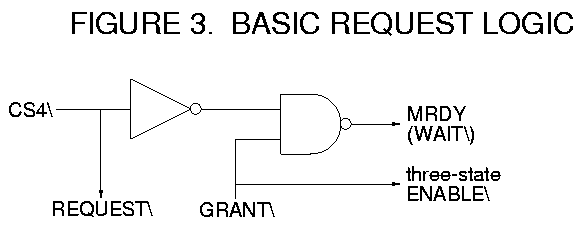
Not so fast! Consider a memory read cycle. In Figure 3, when GRANT\ is asserted, the address and control are enabled onto the external bus, and MRDY is pulled high. But the 6809 interprets MRDY high to mean that the cycle is complete and data is available. There is no time for the memory to respond to the address and output its data!

The circuit in Figure 4 solves this by delaying the low-to-high transition of MRDY. When BUSWAIT\ goes low -- signifying a need for the CPU to wait -- MRDY goes low immediately (because of the active-low CLR inputs on the flip-flops). When BUSWAIT\ goes high, two clocks must occur before MRDY follows (because the high is clocked through two flip-flops). With a 4 MHz clock, this can be a delay of 250 to 500 nsec, depending on when in the clock cycle BUSWAIT\ goes high. Since we're making no assumptions about the Bus Arbiter, we have to assume that GRANT\ is an asynchronous signal -- that is, it can go high anytime during the 6809 clock cycle. Using two flip-flop stages guarantees a minimum of 250 nsec memory access time. Figure 5 illustrates the timing.

We now leap forward to consider a software problem: how do we keep multiple CPUs from altering the same data structure simultaneously? This is the problem of "mutual exclusion" previously described in TCJ [ROD92]. The classic solution is the "semaphore," which works as well for multiple processors as it does for multiple tasks on a single processor...provided that the semaphore operators WAIT and SIGNAL are indivisible.
In a single-CPU system, a semaphore operator can be made indivisible by making it a single machine instruction. The 68000 provides the TAS (Test-And-Set) instruction for this purpose; but a memory rotate or increment/decrement can serve on the 6809 or Z80. The "gotcha" is that this one instruction requires two memory cycles: a read followed by a write. This is commonly called a "read-modify-write" (RMW) memory access: the memory byte is read, a bit is set (modified), and the byte is written back out to memory. Since "modify" takes some time, another CPU could obtain the bus between the read and write...and it's remotely possible that the second CPU would alter the same sempahore during that time. At megaHertz clock rates, even the "remotely possible" occurs too often!
The solution is obvious: the first CPU should not relinquish the bus until it has completed the read-modify-write operation. The REQUEST\ signal must be stretched accordingly. 68000s and 8086s provide a status signal for this purpose. For the 6809 or Z80, we must create our own.
The Z80 is the easier case. We can't necessarily tell when an RMW memory reference is complete, but we can tell when the next instruction begins. The Z80's M1\ signal is pulled low at the start of each new instruction (during opcode fetch).
Figure 6a shows a simple circuit to stretch REQUEST\. When CS4\ goes low (indicating an external access), it clears the flip-flop, forcing REQUEST\ low. Eventually the bus will be granted, releasing WAIT\, and the "read" part of the cycle will occur. During the "modify" part of the cycle, CS4\ may go high, but REQUEST\ will remain low. For the "write," CS4\ will go low again, but -- since this CPU still owns the bus -- GRANT\ is still low, and no wait states will be inserted. When the next instruction begins, M1\ will go low, forcing REQUEST\ back high and releasing the bus.
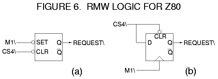
The circuit of Figure 6a will not work if opcodes are being fetched from external memory, since CS4\ and M1\ will be low simultaneously. (This usually will force both flip-flop outputs high.) One fix would use CS4\ to "qualify" the Set input to the flip-flop, so that when CS4\ is low the Set input is forced high. Another fix, (Figure 6b) uses the direct Set/Clear inputs to override the clocked data storage. The rising edge of M1\ will clock the flip-flop high, unless CS4\ is still asserted.
The 6809 doesn't provide a convenient M1\ signal like the Z80. Fortunately, the 6809 is completely deterministic, and its data sheet [MOT83] spells out the cycle-by-cycle execution of each machine instruction. For the shift, rotate, increment, and decrement instructions, the sequence is:
(varying number of cycles to get operand address)
cycle N-2: output operand address, fetch data
cycle N-1: output address FFFF, no data transfer
cycle N: output operand address, store data
where each "cycle" is one cycle of the 6809's E clock. Thus, all read-modify-write operations on the 6809 place one "dead" cycle between the read and the write. So, RMW operations can be made indivisible by stretching REQUEST\ by two extra E cycles.
Figure 7 shows a circuit to do this. This is the same "stretching" circuit used previously, only it is synchronous -- the inputs always change at the same time relative to the E clock. Figure 8 gives an approximate timing diagram.

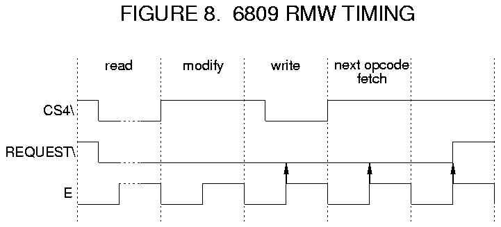
When the read is performed to an "external" address, CS4\ goes low and thus REQUEST\ immediately goes low. This read cycle may be stretched until the bus becomes available. (The E clock will also be stretched.) During the modify cycle, CS4\ will be high and a high level will be clocked into the first flip-flop. Before the high can be clocked into the second flip-flop, CS4\ will be pulled low for the write cycle. CS4\ must remain high for two consecutive cycles before REQUEST\ is de-asserted. This will occur sometime in the next instruction. (Unless, of course, the next instruction also accesses external memory. Note that this logic works properly if instructions are being fetched from external memory.)
The principles described here for the Z80 and 6809 can be adapted for most microprocessors. The CPU must have a WAIT input; thus the 8051 is not suitable. The CPU should have a memory-modify instruction (rotate, shift, or increment/decrement); otherwise, REQUEST\ has to be stretched over several machine instructions, and bus performance will suffer. This makes the 1802 a poor choice.
In the next installment I'll add this logic to the 6809 uniprocessor, design the bus arbiter, and add a few "frills."
[MOT83] Motorola Inc., 8-Bit Microprocessor and Peripheral Data, Motorola data book (1983).
[ROD91] Rodriguez, B. J., "A Z8 Talker and Host," The Computer Journal #51 (Jul/Aug 1991).
[ROD92] Rodriguez, B. J., "Forth Multitasking in a Nutshell," The Computer Journal #58 (Nov/Dec 1992).
A TCJ reader asked why I'm designing with discrete logic instead of PALs. I have several reasons:
1. PALs -- especially 15 nsec or faster -- are still rather expensive. Jameco lists the most basic PALs at $2.50 each, and there is no way I could do the complete 6809 board with fewer than two. On the other hand, my junkbox is well stocked with 7400 series parts and wirewrap sockets.
2. Not everyone is equipped to program PALs. This is especially important for a journal like TCJ, which is trying to make its designs accessible to all readers. I have even had clients specify "no PALs," because they hadn't invested in the development and production hardware. (I, incidentally, do have a little-used PAL programmer.)
3. The logic design is "hidden" inside a PAL. This is aggravated when the minimal or "obvious" logic solution is not the PAL solution (frequently the case). Discrete logic, on the other hand, is easily understandable by any reader of TCJ (I hope).
4. Frankly, using PALs still feels like "cheating" to me. I remember the story told in Soul of a New Machine: when the engineers couldn't solve a hardware design problem, they just put in a block that said "PAL here." It feels like an admission of defeat.
5. I'm a member of the "old school" -- I still take pride in designing circuits with elegance and a minimum of logic. PALs only minimize the number of chips.
6. On the 6809 board, it wouldn't have saved that many chips. Excluding bus buffers and I/O drivers -- which PALs wouldn't replace -- there are only 5 "glue" IC's on the full board. Swapping that for two PALs isn't a great gain.
7. Perhaps most important, TCJ's editor specifically requested hardware articles that didn't use PALs!
Not all of these reasons would be valid in a commercial project. The one-time cost of PAL programmers is trivial for most companies. The added cost of PAL chips is offset by the reduced cost of assembly. "Cheating" to get a design out faster is simply good engineering, and the added flexibility for future design changes alone can justify the use of PALs. But this project is educational, written for impoverished newcomers to digital design. Here, I think discrete logic is best.
Interested in a printed-circuit board for the 6809 multiprocessor? I've been exchanging email with TCJ reader Andrew Houghton, who wants to build a "Poor Man's Transputer" out of the 6809. This prompted some improvement and expansion of the original ScroungeMaster I design. Namely:
a) four RS-485 serial ports using two Z8530s, instead of the 2681
b) two parallel I/O ports, using a 6522
c) memory mapping logic for expanded memory: 32K on board PROM, 32K or 128K on-board RAM, and 384K of off-board (bus) address space
The driving principle is still Cheap Parts: I figure the increased cost of ICs over the ScroungeMaster I is about $9 (Jameco prices). No PALs.
Wire-wrapping one of these boards is enough of a headache -- I'd like to avoid wire-wrapping three more. If we can get commitments for twenty boards, I'll do the PCB layout and get boards fabricated at a local vendor. If interested, send me GEnie mail (B.RODRIGUEZ2), Internet email ([email protected]), or drop a postcard to Brad Rodriguez, Box 77, McMaster University, 1280 Main Street West, Hamilton, Ontario L8S 1C0 Canada.
Note for web publication: the email and postal addresses given above are no longer valid. Contact the author at this email address.