Asynchronous Serial I/O With The PSC1000
Bradford J. Rodriguez, Ph.D.
ABSTRACT
This paper describes a "software UART" for the Patriot Scientific PSC1000 microprocessor. This "soft UART" can simultaneously transmit and receive asynchronous serial data at a programmable baud rate up to 9600 baud, with a programmable number of data bits and stop bits. It uses only the on-chip resources of the PSC1000; in particular, the on-chip bit inputs and bit outputs. It also provides for the continuous refresh of dynamic RAM.
OBJECTIVES
While the Patriot Scientific PSC1000 microprocessor includes a versatile array of on-chip peripherals, a conventional UART (Universal Asynchronous Receiver-Transmitter) is not among them The functions of a UART can be performed in software, using the PSC1000�s Input-Output Processor (IOP) for the precise timing.
A useful "soft UART" must have the following features:
able to simultaneously transmit and receive asynchronous serial data
programmable baud rate
programmable number of data bits and stop bits
uses only the on-chip resources of the PSC1000: CPU, IOP, INTC, bit inputs, and bit outputs
In addition, since the PSC1000 is dependent upon the IOP for dynamic RAM refresh, any IOP program required by the soft UART must also provides for the continuous refresh of DRAM.
ASYNCHRONOUS SERIAL DATA FORMAT
In asynchronous serial transmission, bits are sent one at a time at a fixed rate (the bit rate). The receiver and transmitter do not share a common clock, and it is possible for the their bit clocks to differ slightly (by a few percent at most). To synchronize the receiver to the transmitter, after each transmitted byte, a logic �1� is sent for at least one bit period (the stop bit), and before each transmitted byte, a logic �0� is sent for exactly one bit period (the start bit). The 1-to-0 transition marks the beginning of a new byte of data.
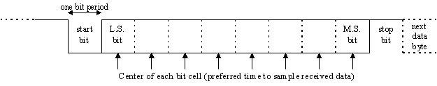
Figure 1. Asynchronous Serial Data Format
Figure 1 illustrates the transmission of an eight-bit "byte" of data. By convention, the eight data bits are sent least-significant bit first. If a parity bit is added, it is sent after the most-significant bit and before the stop bit. Because the bit timing may vary or "jitter" slightly, the receiver should sample the signal line in the center of each bit "cell."
A Universal Asynchronous Receiver-Transmitter (UART) can simultaneously send serial data on one signal line, while receiving different serial data on another line. These two data streams need not be synchronized: a received "incoming" byte can begin at any time, including partway through the transmission of an "outgoing" byte. The edges of the received bit cells are not synchronized with the transmitted bit cells, and may even have slightly different bit periods.
A UART therefore has two independent parts: a serial Transmitter, and a serial Receiver. When given a data byte, the Transmitter must output a start bit, the requisite number of data bits, and one or more stop bits, at a fixed bit rate. The Receiver must detect the edge of the start bit, sample the received data at fixed intervals, and assemble these samples into a received data byte, which is then made available to an application program.
THE PSC1000 SOLUTION
IOP Limitations
The PSC1000�s Input-Output Processor (IOP) is capable of precise and deterministic timing. It can measure a specified interval, and then interrupt the CPU or take some independent action. But the IOP can only time sequential intervals; it cannot time concurrent intervals. In other words, the IOP can perform the function of a single programmable timer.
The I/O capabilities of the IOP are rather limited. It can write the bit outputs only with the OUTT and OUTF instructions, which, respectively, set and reset a specified output pin. It cannot, for example, output a bit from a memory location. It can read the bit inputs only with the TSKIPZ instruction, which causes a change in IOP program flow if an input pin is zero. It cannot read an input to a memory location. Nor can the IOP perform any shifting actions, or any memory reference other than the XFER instruction (which transfers data to or from an external device, not the on-chip peripherals).
In systems containing DRAM, the IOP�s REFRESH instruction causes a refresh cycle to take place. Any IOP program must contain a sufficient number of REFRESHes to ensure that the DRAM refresh requirements are met. A typical requirement is that a complete cycle of 512 refresh cycles be issued at least once every 8 milliseconds. This must be done in addition to any UART timing tasks.
Solution
Given these IOP limitations, some of the functions of the Soft UART must be performed by the Microprocessing Unit (MPU). The Soft UART requires both an IOP program, and an MPU program, working cooperatively. These programs may monopolize the IOP, but must not consume the entire attention of the MPU: it must be possible for the MPU to perform other tasks while serial data is being transmitted and received.
Different solutions are possible, depending on how the UART functions are divided between IOP and CPU, and what options are desired (e.g., fixed or variable baud rate). The solution presented here uses the IOP only to establish the timing for received and transmitted serial data. The IOP interrupts the MPU when it is time to output a new "transmit" data bit, and also when it is time to sample a new "receive" data bit. The MPU�s interrupt routines perform the functions of input, output, bit shifting, and memory access. Thus the tasks of assembling received bits into a byte, and "disassembling" transmitted bytes, are performed by the MPU.
THE IOP TIMING PROGRAM
The IOP program must perform three functions:
Time bit periods for the serial transmitter;
Time bit periods (and half periods) for the serial receiver;
Generate DRAM refresh cycles, even in the absence of received or transmitted data.
Regular intervals can be generated in the IOP with the
DELAY instruction. At first glance, one might think to use a delay of exactly one bit period. But there are two problems. First, the received bit cells are not synchronized with the transmitted bit cells. Receive and transmit bit timing must be concurrent, but independent. Second, an excessively long delay (as would be required for a low baud rate) may cause DRAM refreshes to be generated too infrequently.The solution presented here uses the IOP�s
DELAY instruction to establish an interval which is a fraction of a bit period. This "slice" may be, for example, 1/8 of a bit period. Then a counter can be decremented to wake up the "transmitter" program every 8 slices. Another counter can wake up the "receiver" program every 8 slices. This means that the edges and the center of the bit cell can be resolved to 1/8 of a bit period. With two separate counters, the transmit and receive data need not be "in phase": the receive counter is synchronized to the received start bit, and the transmit counter may be reset whenever transmit data is available.Lower baud rates can be generated by keeping the slice rate unchanged, but increasing the number of slices per bit. The advantage of a fixed slice period is that it becomes much easier to generate the required DRAM refresh: the IOP program need only include the requisite number of REFRESH instructions in each slice period, and this number does not change regardless of the baud rate. Even with very low baud rates, the minimum refresh requirement is guaranteed.
Slice timing
Figure 2 shows the IOP code fragment that establishes the slice interval. The DELAY instruction counts precisely the number of 2X-clock cycles required to fill out a slice period (after refreshing DRAM and decrementing the counters).
This code fragment also illustrates the use of an IOP micro-loop to generate a burst of DRAM refresh cycles. The second instruction group contains three REFRESH instructions and an MLOOP instruction. If the constant iterations is three (for example), nine refreshes will be performed during each slice interval.
The value iterations, and the constant loaded into g7 for the DELAY instruction, depend upon the memory timing of the PSC1000 hardware. They are computed from the desired slice rate at the time the IOP program is assembled.
Transmit bit timing
Once per slice period, the transmit timer decrements a counter, g14. When this counter reaches zero, the MPU is interrupted. The MPU�s interrupt service routine (in this case, for interrupt 4) may then output the next bit to be transmitted. The code for this is shown in Figure 3.
This is an example of time invariant code, which is necessary in the IOP to ensure deterministic timing. Whether or not the counter expires, this code fragment will execute in 3N+1 clock cycles (where N is the number of clock cycles required for an IOP instruction fetch):
If the counter is nonzero: instruction fetch (N cycles), DSKIPZ (1 cycle when the skip is not performed), JUMP (N cycles for instruction fetch at s0_notx), JUMP (N cycles for instruction fetch at s0_tx).
If the counter is zero: instruction fetch (N cycles), DSKIPZ (N cycles for the following instruction fetch, when the skip is performed), INT (1 cycle), JUMP (N cycles for instruction fetch at s0_tx).
Receive bit timing
Similar code is used to generate a "receive bit" interrupt. In this case, the counter is in g13, and interrupt 1 is used. See Figure 4. This again uses an extra jump instruction, to ensure that each path through the code consumes the same number of IOP clock cycles.
Timing of the IOP program
The exact timing of the IOP program depends upon the clock rate of the PSC1000, the Memory Interface timing, and the chosen slice rate. These are all computed automatically when the program is assembled (see the listing in Appendix A). For an 80 MHz processor with a slice rate of 13.02 usec, there will be 1042 2X-clock cycles per slice. The constant iterations will be 1 (i.e., there will be three refreshes per slice). Using typical memory timing, the complete IOP cycle for one slice -- refresh, transmit timing, and receive timing -- will consume 93 2X-clock cycles. The DELAY instruction must wait 949 2X-clock cycles. Thus the "overhead" of the IOP program is 93/1042 or about 9 percent of the available clock cycles.
THE TRANSMIT SERVICE ROUTINE
The Soft UART transmitter must output a �0� start bit, N data bits (LSB first), and one or two �1� stop bits. To simplify the transmit service routine, a word of data is constructed which contains the start bit, data bits, and stop bits, with the start bit as LSB. For example, eight data bits and two stop bits would be encoded as 11xxxxxxxx0. The transmit service routine then simply sends these N+3 bits from the buffer, LSB first.
The MPU is awakened by interrupt 4 when counter g14 expires, indicating that it is time to transmit a new bit. If there are no bits left to be transmitted (indicated by utx_bit_count containing zero), the no_tx_data service is performed. This clears the utx_data buffer, to signal to the application routine that the previous data has been transmitted. It also resets the transmit slice counter to -1 (FFFFFFFF hexadecimal). This has the effect of disabling further transmit interrupts, since the counter will not expire for over 15 hours. (If the counter does expire, it will simply be reset to -1 again.)
If there are bits to be transmitted, the transmit slice counter is reloaded with the value in slices_per_bit (a variable in memory). Then the contents of utx_data are fetched, and the LSB is output on binary output 1. The contents of utx_data are shifted right 1 bit, and stored back into utx_data. Finally, the utx_bit_count value is decremented, indicating the number of bits still to be transmitted.
Note that this interrupt service routine must save and restore the mode register. This is because this register may be altered by the SHR instruction (which affects the GRS bits).
Application Interface
To transmit a byte, the application program must add start and stop bits to the data bits, as described above. The result is stored in utx_data, and the total number of bits (start, data, and stop) is stored in utx_bit_count. Finally, the transmit slice counter, g14, should be set to 1. This will ensure that a transmit interrupt is generated at the next slice interval. When that interrupt is received, the start bit will be output, and the timer reset for the first data bit.
The application program can sense that the transmitter is busy by examining utx_data. If it contains a nonzero value, the transmission of the serial byte is not yet complete. (The high bits of utx_data are set to �1� so that it will contain a nonzero value, even after the final stop bit has been output.)

THE RECEIVE SERVICE ROUTINE
The serial receiver is somewhat more complicated than the transmitter, since it must establish the timing of the incoming data. Figure 6 shows the logic of the receive service routine.
A transition from �1� (stop bit or "idle" state) to �0� always signals the start of a new character. To ensure that this is a valid start bit, and not a momentary glitch on the input line, the receiver delays for one-half a bit period -- to the center of the bit cell -- and then samples the input pin again. If this is a valid start bit, the input will still be zero.
The receiver then samples the input data at the center of each bit cell. This is the best time to sample the incoming bits, since it offers the greatest immunity from errors in bit timing (due to "jitter" or a slightly inaccurate baud rate). Having already delayed to the center of the start bit, the receiver need only delay one full bit period to the center of each successive bit cell.
This requires three actions in the PSC1000:
Detect the edge of the start bit;
Check the center of the start bit;
Read serial data from the center of the bit cell.
This involves three separate interrupt service routines, which are selected by changing the address in the interrupt vector.
Start bit detection
The PSC1000�s Interrupt Controller (INTC) is ideally suited to detecting the leading edge of the start bit. When the bit input is so enabled, a �0� input will generate an interrupt request to the MPU.
Initially, the binary input interrupt is enabled while the input is �1�, during the stop bit or the idle time between bytes. The transition from �1� to �0� causes an immediate MPU interrupt. The MPU�s interrupt service routine (Figure 7) then disables the input interrupt, and starts the "timer" interrupt by storing a value (one-half the number of slices required for one bit) in the receive slice counter. When the IOP counts this many slices, it will interrupt the MPU again.
In this example, both the INTC and the IOP use the same interrupt to signal the receive service routine. Since they use the interrupt at different -- and mutually exclusive -- times, there is no conflict.
Start bit checking
Halfway through the start bit, the MPU is interrupted by the IOP. The MPU must then test the input to ensure that this is a valid start bit.
Whenever the MPU reads the serial input, it must circumvent the zero persistence. This is a characteristic of the PSC1000�s binary inputs, by which any �0� detected on the input line is latched until the bit is consumed.
For example, suppose that a false start bit, 1/8 of a bit period in duration, were received. The leading edge of the false start would interrupt the MPU (as previously described). After the interrupt service completes, the input pin will still be zero; but sometime while the IOP is timing the half-bit interval, the input pin will go high. This 0-to-1 transition will be ignored by the binary input. When the IOP interrupts the MPU, the �0� input will still be latched in the input register.
Therefore, before sampling the binary input, its persisting zero must be released. This is done by writing a �1� to the desired bit of the input register, as shown in Figure 8.
If the input pin is �1�, indicating a false start bit, the MPU returns to the "wait for start bit" state by resetting the interrupt vector and re-enabling the INTC. If the start bit is valid, the MPU sets the IOP�s receive slice counter to the number of slices for one full bit period, changes the interrupt vector to the "receive bit" service routine, disables the INTC, and initializes the memory variables used for data reception. (Refer to the code in Appendix A.)
Receive bit sampling
For each of the subsequent data bits and stop bits, the IOP interrupts the MPU in the center of a bit cell. The MPU reads the input bit, taking the same precautions for zero-persistence just described. This input is shifted right into urx_data.
After the stop bits have been sampled, the MPU can return to the "wait for start bit" state. At first glance, one might think the MPU could reset the state machine after the last data bit was sampled. But this sampling occurs in the center of the bit cell, and if the last data bit is zero, the INTC would be re-enabled while the input pin was zero, falsely interpreting the final data bit to be a start bit. Rather than create a separate receive state to delay into the stop bit, the MPU simply samples the stop bit as though it were a data bit.
When a complete byte has been assembled, it is copied from the receive "shift register" urx_data, into a separate variable urx_buffer. This frees the shift register to accept new serial data immediately, while the application program is processing the byte just received.
While waiting for the next start bit, the receive slice counter will continue to decrement. If sufficient time elapses with no start bit detected, it will decrement from FFFFFFFF down to zero and generate a receive interrupt. In this case, the input pin is still �1�, so this interrupt will be rejected as a false start bit and the counter will resume decrementing from FFFFFFFF.
If a "break" condition is present, the serial input line is held at �0�. As soon as the MPU awaits a start bit, the input interrupt will be asserted (because the input is zero) and a new byte will be received. Thus a break condition will be seen as a continuous stream of null characters.
Refer to Appendix A for the complete receiver program.
ERROR DETECTION
Framing errors and breaks
Since the stop bits are stored along with the data bits in the receive data register, the application program can examine them for error conditions. For a correctly received byte, the stop bit(s) should be �1�. If a data byte has one or more �0� stop bits, a framing error has occurred.
Similarly, a break condition (input held at �0�) will appear as a null data byte with �0� stop bits. As long as the break condition is present, nulls will continue to appear in the receive data register. When the break condition ends (input returns to �1�), one spurious character with an unknown number of zero bits may remain in the receive data register.
Parity
The Soft UART code presented here does not generate or check parity. Transmitted parity can be generated from the application program, and received parity can be returned to the application program, by treating the parity as an additional data bit.
For example, to use 8 data bits with parity, the Soft UART should be programmed to send and receive 9 data bits. The parity bit is the most significant bit. For transmitted bytes, the application can use a lookup table or a bit counting algorithm to determine the parity of the character, and the parity bit can be set or cleared as necessary to produce an odd or even number of �1� bits in the transmitted data. The same lookup table or algorithm can be used to determine the parity of received characters, and this can be compared with the expected (odd or even) value.
9th-bit wake-up
Some UARTs support 9 bits of serial data, with the 9th (most significant) bit being as a "wake up" flag. This is typically used for bussed multidrop networks, having several receivers listening to the same data stream, and with blocks ("frames") of data being addressed to specific receivers. The 9th "wake up" bit is used to indicate that the byte is a destination address, and all receivers should wake up and examine this byte. The designated receiver destination recognizes its own address, and enables the UART to receive all following characters (the rest of the frame). The other receivers can "go to sleep" and ignore the subsequent serial data, until another "wake up" is detected, signaling the start of the next frame.
The code presented here supports 9-bit data, but does not include a specific wake-up function. In other words, all received characters will be stored and returned to the application, but the application can examine the received characters for the "address mark" which denotes the beginning of a frame.
THE C PROGRAMMING INTERFACE
The application program uses four C functions to initialize, transmit, and receive serial data:
void init_uart(int baudrate, int databits, int stopbits) initializes the Soft UART to the given baud rate, number of data bits, and number of stop bits. Any baud rate less than the slice rate can be specified, but the nearest submultiple of the baud rate will be used. For best results the baud rate should be no greater than 1/8 the slice rate. Any number of data bits and stop bits can be specified, as long as the total is less than 31.
int uart_tx(int c) puts the character �c� in the transmit data buffer and starts the transmitter. The programmer must use uart_txready to ensure that the buffer is empty before calling uart_tx. The returned value is the character �c�. Characters larger than 8 bits are supported if the Soft UART has been so initialized.
int uart_txready() returns true (nonzero) if the transmitter is empty and can accept a character. Outputting a character when the transmitter is not ready may have unpredictable results.
int uart_rx() returns false (zero) if no character has been received by the Soft UART; otherwise returns the character. The data bits are the least significant bits of the returned value, followed by the received stop bit(s). The receiver is double-buffered, so uart_rx will return a valid result until another entire character is received by the Soft UART. Uart_rx performs a destructive read of the character, so subsequent calls to uart_rx will return zero until a new character is received.
LIMITATIONS
The Soft UART can only be used for low to moderate baud rates. The principal limitation is the requirement that the IOP "wake up" eight times (or more) per bit period, and decrement and test two counters. As mentioned previously, on a typical PSC1000 system, a slice rate sufficient for 9600 baud causes the IOP to consume about 9% of the available processor cycles. Increasing the baud rate to 38400 baud would require quadrupling the slice rate, and the IOP would be expected to consume 36% of the processor cycles.
There is also an MPU overhead incurred by the interrupt service routines, but this is significantly less because it occurs only once per bit.
The code presented here buffers only one received character, and must be polled by the application. If the application does not call uart_rx frequently enough, a receive overrun can occur and data can be lost.
FURTHER REFINEMENTS
This code is presented to illustrate how the IOP, MPU, and INTC can be used to send and receive serial data. It has been kept simple for illustrative purposes. Several improvements can be made to the IOP or MPU programs, which would make the Soft UART more useful for some applications.
Stop bit detection
The stop bit(s) are currently presumed to immediately follow the data bits. No attempt is made to verify that the stop bit is truly in the �1� state. As a consequence, a break condition (steady �0�) on the bit input will be interpreted as a continuous stream of null characters, rather than a single break. To solve this problem, the MPU�s receive service routine could be modified: after the data bits have been received, continue to sample the input once per bit period (in the center of the bit cell) until a �1� input is detected. As long as the input is �0�, the invalid stop bits should be discarded.
Receive buffer
The single-buffered receiver requires that the application poll the receiver at least once per byte period (approximately once per millisecond at 9600 baud). Complex applications may be involved in other tasks for periods exceeding a millisecond, causing characters to be lost. A circular buffer for received characters (FIFO) of 256 or even 16 bytes would greatly alleviate this problem. The receive service routine, instead of copying the received character to a memory cell, would append it to the circular buffer; then the uart_rx routine would fetch the next character (if any) from that buffer.
Parity
If the application will send and receive serial data with parity, it would be worthwhile to add parity checking to the Soft UART. This can be done as part of the uart_tx and uart_rx routines. (A fourth parameter can be added to the init_uart routine, to select odd, even, mark, space, or no parity.)
Wake up function
If the application will be using the 9th data bit for "address mark" wake-up, the receive service routine can be modified accordingly. A status flag can indicate receiver "active" or "inactive." While in the "inactive" state, received characters are discarded unless the 9th bit is set. When the 9th bit is detected, the receiver is switched to the "active" state, and all subsequent received characters are stored in the buffer or queue. A new function must be added to allow the application to switch the receiver back to the "inactive" state.
REFERENCES
1. Shaw, George William. PSC1000(tm) Microprocessor Reference Manual. Patriot Scientific Corporation, 1998.